Random Number Generator


Materials :
This project has been a wonderful experience and like all projects it's had its ups and downs. Right off the bat I had some difficulties with my soldering iron, which simply refused to become hot enough to work. Two more soldering irons latter and I finally could start my work. After this problem was assuaged I was soldering like a champ and the 7 180 ohm resistors were affixed.Next up were the 7 red LEDs which i took care of as well making sure that the longest lead (positive) was placed in the square hole. This was the end of day one of my work with the soldering iron.
- 180 ohm resistors (7)
- 1.2k ohm resistor
- 10k ohm resistor
- Red LEDs (7)
- 100 microferad capacitor
- .47 microferad capacitor
- .01 microferad capacitor
- Push button switch
- Slider switch
- 555 timer
- 74LS74 (Integrated circuit)
- 74LS74 (Integrated circuit)
- 74LS04 (Integrated circuit)
- 74LS32 (Integrated circuit)
- 74LS08 (Integrated circuit)
- Circuit board
- 14 pin sockets (5)
- 8 pin sockets (5)
- Battery holder
- Solder
- Soldering iron
- Wire Cutters
- Iron holder
- Sponge
This project has been a wonderful experience and like all projects it's had its ups and downs. Right off the bat I had some difficulties with my soldering iron, which simply refused to become hot enough to work. Two more soldering irons latter and I finally could start my work. After this problem was assuaged I was soldering like a champ and the 7 180 ohm resistors were affixed.Next up were the 7 red LEDs which i took care of as well making sure that the longest lead (positive) was placed in the square hole. This was the end of day one of my work with the soldering iron.
Goal:
The goal of the project was to create a working device that randomly generated numbers through the use of LEDs. In order to do so we had to take inventory of all the necessary parts and then place them correctly in their positions.Once we found a part's place we used a soldering iron to affix it.
Reflection:

Now day two I managed to work without any issues occurring, and thus I was able to put in the remaining resistors, all the capacitors and both switches. I made sure to be especially careful that I put the positive lead of each capacitor into the hole marked with a plus sign.

On day three I managed to attach the 14 pin and 8 pin sockets as well as the battery holder. However due to the fact that I was rushing to attach the battery holder before the bell rang I somehow managed to put it on backwards. This I corrected on my fourth day of work after I put on the integrated circuits, by using the solder sucker. After this I tried it out and however it did not work properly so I corrected this but getting rid of a bubble in the one of the spots I soldered. This fixed the problem
Majority Vote
The goal of this project was to create a circuit that would be able to simulate a voting process. We were to first to create a logic expression, truth table and a circuit. From there we simplified our logic expressions and circuits, and finally created the circuit on a breadboard.
Truth Table
The purpose of a truth table is to show all the possible outcomes for a circuit based certain components being on or off. It uses ones and zeros to show whether a component is off or not.

In this table there are 4 components (P, V, S, T) that determine the outcome (D). Each component can either be on (1) or off (0), which means that each component needs 2 rows, since there are 4 different components I took 2 to the 4th power and got 16 rows. The table shows using ones and zeros that when the majority vote yes the decision passes, likewise when the majority vote no it does not pass. It also shows that when there is a tie the President has the deciding vote so if he votes yes it passes, if he doesn't it does not.
Un-simplified Logic Expression

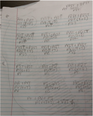
The logic expression above tells you that when the President votes no and the other three votes yes then the movement passes. If the President and Treasurer vote yes and the other no then it passes because in the case of a tie the president's vote decides it. If the President and Secretary votes yes then it passes. If everyone except for the Vice President votes yes then it passes. If the President and Vice President vote yes then it passes. If everyone except for the Secretary votes yes then it passes. If everyone except for The Treasurer votes yes then it passes. Finally if everyone votes yes then obviously the majority vote is yes. This is a sum of Products form because it takes each min term and adds it. I got each min term by looking at my table and the ones with an outcome of 1 I wrote a min term for using the not symbol to represent zeros. I chose to use SOP form instead of POS form because it was more easily written with the information I had.
Un-simplified Circuit
The image below represents the un-simplified version of the circuit. It uses 2 input NOT gates, 2 input And gates, and 2 input OR gates to simulate the majority votes.
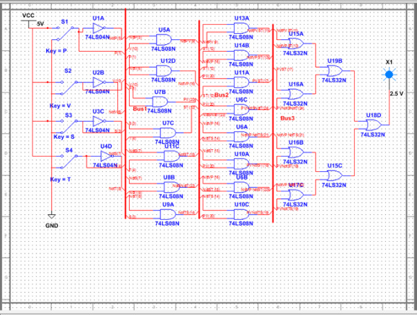
The circuit above is currently in bus form. It took 4 NOT gates, 15 AND gates, and 6 OR gates.Since it needed so many gates it also needed many chips. It would have taken 1 74LS04 chip, 4 74LS08 chips, and 2 74LS32 chips. If we had to create this it would be far to complicated and costly, so instead we simplified it getting rid of all unnecessary gates.
Simplified Logic Expression
The expression tells me that whenever the president votes yes and at least one other member votes yes the decision is yes. Also if at least 3 member votes yes then the decision is yes
P (V + S + T)
+ V + S + T
Simplified Circuit
The circuit below uses AND gates and OR gates to create the same scenario as the un-simplified circuit. However it is much less cramped because the simplified logic expression told us that the NOT gates were unneeded as well as many of the other gates.

The circuit is currently in bus form like the one before it. There are 5 AND gates , and 3 OR gates required to make this circuit. This transfers over to 2 74LSo8 chips, and 1 74LS32 chip. I figured this out because each chip contains 4 gates, this being the case I knew I needed 1 chip for every 4 gates of the same type.
The simplified circuit definitely contained fewer gates than its un-simplified counterpart. This being the case it also had fewer chips. To be exact it contained 4 fewer gates. This is important because it is far more cost and time worthy, because it means fewer parts to buy and less parts to connect saving you from a confusing jumble of wires.
The simplified circuit definitely contained fewer gates than its un-simplified counterpart. This being the case it also had fewer chips. To be exact it contained 4 fewer gates. This is important because it is far more cost and time worthy, because it means fewer parts to buy and less parts to connect saving you from a confusing jumble of wires.
Bread Boarding
The list below describes what parts and how much of each was used.


This picture shows the CDS which contains all the necessary parts needed like the switches. However it did not contain the chips, wires, resistor or LED.

This picture shows you just how many wires are necessary to hook everything up properly.

This shows how each part was placed and gives you an idea of how they are connected.
My first experience breadboard was not a total disaster however at times it did try on my patience. It makes you be very detail oriented because misplacing a single wire or forgetting to hook something up can spell disaster for you. For example a few times I realized that one of my wires had come loose when I was trying to attach something else. Also towards the end it came to my attention that the leg of one of my chips had been bent and caused my whole circuit to stop working. However I must say that it certainly could have been worse so I won't complain.
Conclusion
This project like the one before it had its ups and downs. In the beginning the project was fairly simple; I simply had to look at the conditions that needed to be met and create a truth table from that information. After that I needed to write an un-simplified logic expression which I did without much trouble. The next step was a little trickier I had to create a circuit in multi sim using my un-simplified expression. The issue I had with this was being able to connect the gates to the bus correctly, which was quite a task. After I did this I had to simplify the logic expression, this was difficult because with all the variables it is easy to miss or combine them wrong. Also there were the lines above variables certain variables which could easily be lost as well, systematically making your whole equation wrong. Once I had finished this however creating the simplified circuit was simple. When I was done with the circuit I just had to recreate it on the bread board. This was not too hard a task save for the fact that I had a bent leg on one of my gates which had me looking at my circuit for a while before I realized that it was the culprit. Though I had some mishaps along the way I have realized the complexities and importance of this project, that even though parts may be frustrating they have a purpose. For example without Boolean algebra designing circuitry would be far more confusing and costly, so I begrudgingly must appreciate its existence.
Date of Birth
Overview:
The purpose of this project was to create a circuit that would show our birth dates in a seven segment display. We used K- Maps and a truth table to create a simplified logic for our circuit. For this circuit we had to use a common cathode seven segment display, a NOR gate and a NAND gate, the rest was up to us to design.
The purpose of this project was to create a circuit that would show our birth dates in a seven segment display. We used K- Maps and a truth table to create a simplified logic for our circuit. For this circuit we had to use a common cathode seven segment display, a NOR gate and a NAND gate, the rest was up to us to design.

Truth Table
The chart below is a truth table describing the out comes of different input combinations. It tells you what number should appear when certain switches are turned on or off. It also tells you which sections of the 7 segment display are on in order to create the number on the display.

The first three columns of the table represent each of the 3 switches that control the circuit, when there is a zero the switch is off, when there is a one then it is on. The column named display shows you what number is supposed to appear on the 7 segment display if those conditions seen before it are met. The columns A-G represent each of the seven segments on the 7 segment display. When there is a zero the segment is not powered, if there is a one it is. The X's on the table tell you that that part does not matter to the outcome so it could be either a zero or a one.
K- Maps and Simplified Logic
K-Mapping is a method of simplifying an expression other than Boolean Algebra. K-Maps use the output column of truth tables to simplify, it breaks the zeros and ones into groups of 2 or 4 based on how many different variables there are. The groups are then placed in their own rows in the K-Map. In this case they were split into twos, the first two went in the first row, the next went into the second making sure to keep the same order. The third group goes into the last row, and the fourth group goes into the third row. As for labeling the first two variables go on the side, the last go on top. There are four variations for the side and 2 for the top. For the side the first two variables are both NOTs, for the next row just the first variable is NOT, for the next none of the variables are NOT, and finally for the last only the second variable is NOT. For the top only the first variable in the first column is NOT. Now to simplify you have to group the ones into groups of 1,2, 0r 4. When you have grouped everything you create a SOP logic expression for it with each part corresponding to a group on the K-MAP. Make sure when doing this that if the ones in a group have the same variable that you exclude it from the expression only include a variable if it differs from the others describing the grouping. Also if there is an X it can act as a 1 if needed to complete a group. K-Mapping is a better choice than Boolean Algebra for simplifying a logic expression because unlike Boolean it is not as easy to make as mistake such as misplacing or mistaking a variable. Also you don't need to worry about when to stop simplifying. There are so many expressions in this situation because each one describes a different segment of the 7 segment display.


Circuit
The circuit below shows how I used NOT, AND, OR, NAND & NOR gates to create my birthdate in the 7 segment display. Each segment of the 7 segment display is connected to the gates which combine to create the simplified logic expressions we found earlier.

First I connected the switches to power and ground, and then connected it to a bus, as well as NOT gates. Then we connected the NOT gates to the bus as well. Next I used the appropriate gates and connected them to the bus, these gates I then connected with others and then the corresponding segment of the & segment display. Finally I connected the 7 segment display to a ground since it is a common cathode. The circuit required 2 OR gates, 1 AND gate, 5 NAND gates,2 NOR gates and 3 NOT gates. It would take 1 74LS04 chip, 1 74LS32 chip, 1 74LS08 chip, 2 74LS00 chips, and 1 74LS02 chip. I used NAND and NOR gates for the segments I did because I thought that they would be the easiest ones to use. We use NAND and NOR gates because they make it so that we can use fewer chips because we don't have to use as many kinds of chips. Circuits with NAND and NOR gates may use more gates in some situations, however it uses fewer chips. For my NOR circuit it uses 1 more gate but it means I use fewer chips total. My NAND circuit uses more 2 more gates, but fewer chips. Using more gates means that it will not work quite as quickly however it saves, space and money when creating a circuit. A seven segment display, as the name hints, has 7 segments named A-G. Depending on whether it is common cathode or anode it is connected to ground or power. Then if its a common cathode you connect the ones you want powered to power and if anode to ground. the LEDs will only turn on if they are connected to both ground and power. We used a common cathode version because we used switches which were connected to power. The purpose of the resistor before the display was to regulate the flow of current.
Materials
The purpose of the table below is to illustrate what materials we used and the quantities of each.

Bread Boarding

Here you can see in the bottom left corner the two wires connecting the main board to power and ground. You can also see wires connecting chips as well as powering and grounding the chip.

In this picture you can see where I connected the main board to the switches and the number 7 appearing on the display.

This is a picture of the final product in which you can see all the chips connected and the display working.
My second bread boarding experience was a little bit easier for me than the last. I no longer made trivial mistakes such as not grounding or powering the chip, or placing a wire in the wrong area. However there were still some issues when we were about three quarters of the way through we realized that our birth dates would not work in the circuit the way we originally had them, so we instead used Terrie's birth date which was simpler and worked. After that it wasn't too hard however I was mistaken on the layout of one of the chips and had to fix it. The only issue other than that was wires accidentally falling out.
Conclusion
During the conception of this project I learned about the processes involved in K-Mapping, NAND and NOR circuits, and using seven segment displays to create a working circuit. If I were to do this project over again I would use a simpler date so that I would not have to change designs part way through bread boarding. I would also print out pictures describing the insides of all the chips. I believe that I need a little more practice with K-Maps before I have conquered them. K-Mapping is useful because it allows for a quicker simpler way to simplify logic expressions.
Copier Jam Detector

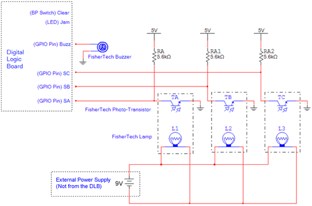
The problem we are trying to simulate below is that of a jammed copy machine. In our device when two adjacent lights were covered it simulated a jam in the machine. This jam would set off a LED light and buzzer signaling that there was a malfunction in the system.
Project Statement
For this project we used the Field Programmable Gate Array on the Digital Logic Board to design a combinational logic circuit that will monitor the copier's three input sensors and activate both an LED and an audio buzzer whenever a paper jam is detected. the inputs from the three sensors (SA, SB, and SC) and the output to the buzzer should be connected to four of the Digital Logic Board's general purpose I/O input pins. The Clear signal should be connected to any of the Digital Logic Board's four pushbutton switches. The Jam signal should be connected to any one of the Digital Logic Board's eight LEDs.
Constraints
When a paper jam occurs, an LED indicator light will turn on and a buzzer will sound. The LED indicator will go off as soon as the jam is cleared. The buzzer should continue to sound until a reset button is pressed. this last condition requires that the output controlling the buzzer be latched with a flip-flop. We could also only use AOI logic to create our circuits.
Truth Table

Unsimplified Logic Expression

Boolean Algebra

K- Mapping


Wiring Diagram
MultiSim

Wiring

Explanation
In this design there are three lights and three photo transistors. When the light from two adjacent lights is stopped from reaching the transistors it registers and sets off the LED. It also goes through the flip flop which holds the signal and to the buzzer, when the clear button is hit (BTNO) it goes through the inverter and flip flop and shuts the buzzer off. In this design the transistors acted as inputs. Some other examples of inputs are microphones, controllers and scanners. The PLD mode allows you to create circuits without using chips but instead using a circuit you designed online and uploaded onto the device. This method is definitely easier than the other because it lets you use fewer parts and wires and takes less time to construct. A problem we came across when doing this was that our device was not connected to the program, so we had to connect it manually. The purpose of the buzzer was to notify you of a jam in a way that was easily discernible. The buzzer stayed on until cleared because it went through the flip-flop which holds the signal until it changes via the button, where the LED did not have to pass through the flip-flop device.
Conclusion
In order to create this project a variety of different concepts were used. These concepts include truth tables, minterms, Boolean Algebra simplification, K-map simplification, logic expression, the PLD mode on MultiSim, AOI logic, and flip-flop (latch).Truth tables are used to show all the possible outcomes of a circuit, using ones and zeros. Minterms show what can be on or off in a circuit in order for the outcome to be equal to one. Boolean Algebra is used to simplify logic expressions. K-mapping is another method for simplifying logic expressions that turns a truth table into a grid where it groups together ones into 2's, 4's, and 8's. A logic expression is an expression using variables to show which variables need to be on or off in order to get the outcome that you want. It uses inverter logic to turn a variable off so that its not on and OR logic to show that more than one combination can result in the outcome you want, and finally it uses AND logic to show that more than one variable needs to be involved to get your desired outcome.The PLD mode on multisim allows you to upload a circuit onto a Digital Logic Board, so that you do not have to use logic chips. AOI logic stands for AND, OR, & Inverter logic. This logic is used to combine or change the variables involved to create a logic expression or a circuit. Finally a flip-flop (latch) is used to hold a signal constant until something changes it such as the clearing button on our circuit.
